
Entrar
insight - Optics and Photonics - # Singular Dielectric Nanolaser with Atomic-Scale Field Localization
Dielectric Nanolaser with Atomic-Scale Field Localization Breaks Optical Diffraction Limit
Conceitos Básicos
Dielectric nanolasers can achieve optical field confinement beyond the diffraction limit, enabling ultra-precise measurements, super-resolution imaging, and exploration of light-matter interactions at the atomic scale.
Resumo
The content discusses the development of a singular dielectric nanolaser that can compress the optical field to the atomic scale, breaking the fundamental constraint imposed by the diffraction limit. Unlike plasmonic structures, which suffer from inherent ohmic loss, the proposed dielectric nanolaser leverages the divergence of momentum derived from Maxwell's equations to achieve superior field confinement.
The key highlights are:
- Compressing the optical field to the atomic scale opens up new possibilities for directly observing individual molecules and enabling innovative imaging and research tools.
- The researchers discovered that the electric-field singularity sustained in a dielectric bowtie nanoantenna originates from the divergence of momentum, as derived from Maxwell's equations.
- The singular dielectric nanolaser is constructed by integrating a dielectric bowtie nanoantenna into the center of a twisted lattice nanocavity, which synergistically surpasses the diffraction limit.
- The singular dielectric nanolaser achieves an ultrasmall mode volume of about 0.0005 λ^3 (λ, free-space wavelength) and a feature size at the 1-nanometer scale, enabled by a two-step fabrication process involving etching and atomic deposition.
- This research showcases the ability to achieve atomic-scale field localization in laser devices, paving the way for ultra-precise measurements, super-resolution imaging, ultra-efficient computing and communication, and the exploration of light-matter interactions within the realm of extreme optical field localization.
Personalizar Resumo
Reescrever com IA
Gerar Citações
Traduzir Texto Original
Para Outro Idioma
Gerar Mapa Mental
do conteúdo original
Visitar Fonte
www.nature.com
Singular dielectric nanolaser with atomic-scale field localization - Nature
Estatísticas
The singular dielectric nanolaser achieves an ultrasmall mode volume of about 0.0005 λ^3 (λ, free-space wavelength).
The singular dielectric nanolaser has a feature size at the 1-nanometer scale.
Citações
"Compressing the optical field to the atomic scale opens up possibilities for directly observing individual molecules, offering innovative imaging and research tools for both physical and life sciences."
"Our research showcases the ability to achieve atomic-scale field localization in laser devices, paving the way for ultra-precise measurements, super-resolution imaging, ultra-efficient computing and communication, and the exploration of light-matter interactions within the realm of extreme optical field localization."
Principais Insights Extraídos De
by Yun-Hao Ouya... às www.nature.com 07-17-2024
https://www.nature.com/articles/s41586-024-07674-9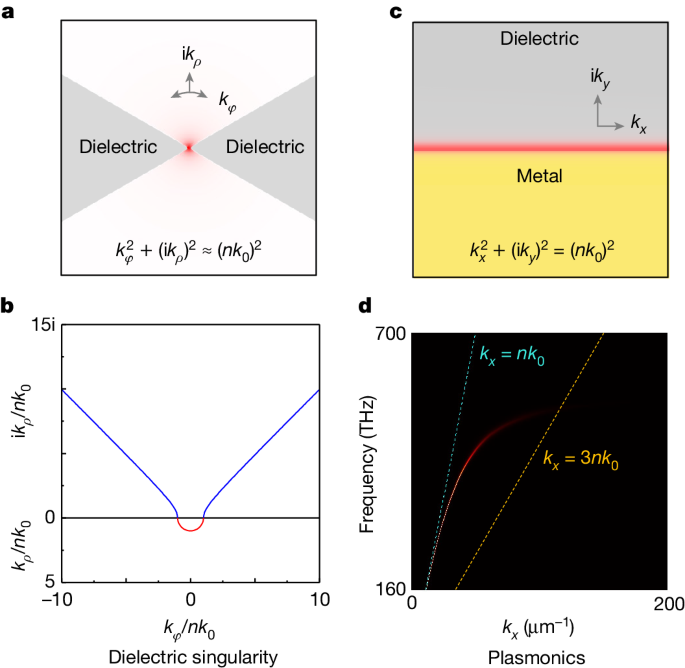
Perguntas Mais Profundas
What are the potential applications of the singular dielectric nanolaser in fields beyond physical and life sciences, such as quantum computing or energy harvesting?
The singular dielectric nanolaser holds immense potential in various fields beyond physical and life sciences. In quantum computing, these nanolasers could be utilized for quantum information processing, enabling ultra-precise manipulation of quantum states due to their atomic-scale field localization. Moreover, in energy harvesting applications, these nanolasers could enhance the efficiency of photovoltaic cells by providing highly localized light sources for improved energy conversion.
How can the fabrication process be further optimized to improve the reliability and scalability of the singular dielectric nanolaser?
To enhance the reliability and scalability of the fabrication process for singular dielectric nanolasers, several optimizations can be implemented. One approach is to refine the etching and atomic deposition techniques to achieve even greater precision in creating the required dielectric bowtie nanoantennas with single-nanometre gaps. Additionally, advancements in nanofabrication technologies such as electron beam lithography and focused ion beam milling can be leveraged to further improve the reproducibility and scalability of manufacturing these nanolasers.
What are the fundamental limits of optical field confinement, and how might future advancements in materials and device engineering push the boundaries of what is possible?
The fundamental limits of optical field confinement are primarily dictated by the diffraction limit, which restricts how tightly an optical field can be focused. However, advancements in materials science and device engineering offer avenues to push these limits further. By exploring novel dielectric materials with tailored optical properties, such as metamaterials or quantum dots, researchers can potentially achieve even tighter field confinement beyond what is currently possible. Moreover, innovative device designs and integration of plasmonic elements could lead to breakthroughs in surpassing existing boundaries of optical field confinement, opening up new possibilities for applications in nanophotonics, quantum optics, and beyond.
0
Produtos
© 2024 by Linnk AI