toplogo
Entrar

Rapid X-ray Imaging Reveals Intricate Details of Microchip Transistors


Conceitos Básicos
Rapid X-ray burst imaging can map the internal structure of computer chips with unprecedented 4-nanometer resolution, enabling new insights into the complexity of modern microchips.
Resumo

The article discusses a new method for non-destructively imaging the internal structure of computer chips using rapid X-ray bursts. Current microchip fabrication techniques can pack around 50 billion transistors onto a chip the size of a fingertip, enabling innovations in artificial intelligence and augmented reality. However, imaging these intricate circuits in 3D has remained a challenge.

The researchers developed a technique that can map the integrated circuits inside chips with a record resolution of 4 nanometers, up to 170 times faster than existing methods. This allows for detailed, non-destructive visualization of the complex transistor layouts and interconnects within modern microchips. The rapid X-ray bursts enable high-speed imaging that can capture the chip's internal structure without damaging the device.

This breakthrough in chip imaging technology provides new opportunities to study and optimize the design of integrated circuits, which are critical components powering a wide range of modern electronic devices and emerging technologies. The ability to rapidly and non-invasively inspect the internal structure of microchips at the nanoscale level can lead to important insights for improving chip performance, power efficiency, and reliability.

edit_icon

Customize Summary

edit_icon

Rewrite with AI

edit_icon

Generate Citations

translate_icon

Translate Source

visual_icon

Generate MindMap

visit_icon

Visit Source

Estatísticas
Chips can contain around 50 billion transistors in a fingertip-sized area. The new X-ray imaging method achieves a resolution of 4 nanometers, up to 170 times faster than existing techniques.
Citações
"Such techniques are making computer chips more complex, powerful and efficient than their predecessors — enabling innovations that are essential for artificial-intelligence and augmented-reality technologies." "Rapid X-ray burst imaging can map the internal structure of computer chips with unprecedented 4-nanometer resolution, enabling new insights into the complexity of modern microchips."

Principais Insights Extraídos De

by Tais Gorkhov... às www.nature.com 07-31-2024

https://www.nature.com/articles/d41586-024-02377-7
Microchip minutiae imaged using rapid X-ray bursts

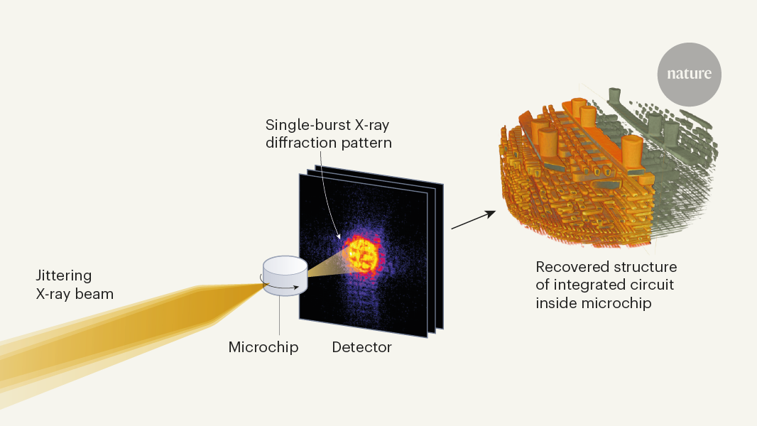
Perguntas Mais Profundas

How can this rapid X-ray imaging technique be leveraged to accelerate the development and optimization of next-generation microchip designs?

The rapid X-ray imaging technique described in the context can significantly accelerate the development and optimization of next-generation microchip designs in several ways. Firstly, the ability to map integrated circuits inside chips in 3D with a resolution of 4 nanometres allows for a detailed analysis of the chip's structure, identifying any defects or areas for improvement. This level of precision enables engineers to fine-tune the design for better performance and efficiency. Moreover, the speed at which this imaging technique operates, up to 170 times faster than existing methods, means that designers can quickly iterate on different chip configurations and test their impact without significant delays. This rapid feedback loop can lead to faster innovation cycles and ultimately expedite the time-to-market for new microchip technologies.

What potential limitations or challenges might arise in scaling this imaging method to larger or more complex integrated circuits?

While the rapid X-ray imaging technique offers unprecedented resolution and speed for visualizing microchips, scaling this method to larger or more complex integrated circuits may present certain limitations and challenges. One potential limitation is the computational complexity involved in processing the vast amount of data generated by imaging larger chips. As the size and complexity of the integrated circuits increase, the computational resources required to reconstruct and analyze the 3D images also grow significantly. This could lead to longer processing times and potentially bottleneck the imaging process. Additionally, the physical constraints of X-ray imaging, such as the penetration depth and scattering effects, may pose challenges when imaging larger chips with multiple layers of circuitry. Ensuring that the X-ray beams can penetrate through the entire structure and accurately capture the details of each layer becomes more challenging as the size of the chip increases.

What other emerging technologies or scientific fields could benefit from the ability to non-destructively visualize nanoscale structures with such high resolution and speed?

The ability to non-destructively visualize nanoscale structures with high resolution and speed, as enabled by the rapid X-ray imaging technique, has the potential to benefit various emerging technologies and scientific fields. One such field is nanotechnology, where precise imaging of nanostructures is crucial for understanding their properties and behavior. By visualizing nanoscale structures in 3D with a resolution of 4 nanometres, researchers can gain valuable insights into the atomic arrangement and interactions within these materials, leading to advancements in nanomaterials design and applications. Additionally, fields such as biotechnology and materials science could benefit from this imaging capability to study biological samples, polymers, and other complex materials at the nanoscale. The high resolution and speed of the imaging technique open up new possibilities for studying dynamic processes and interactions at the molecular level, driving innovation in various scientific disciplines.
0
star