
Sign In
insight - Computational Complexity - # Ultrafast All-Optical Microscopy for Atomic-Scale Imaging and Dynamics
All-Optical Microscopy Achieving Picometric Spatial and Femtosecond Temporal Resolution for Probing Atomic-Scale Dynamics
Core Concepts
Leveraging extreme atomic nonlinearities, the authors have developed an all-optical microscopy technique that achieves picometric spatial and femtosecond temporal resolution, enabling direct monitoring of quantum light-matter interactions and electronic dynamics at the atomic scale.
Abstract
The content describes a breakthrough in optical microscopy that pushes the boundaries of spatial and temporal resolution to the atomic scale. The authors have developed an all-optical microscopy technique that exploits extreme atomic nonlinearities within tip-confined evanescent fields to achieve picometric (trillionths of a meter) spatial and femtosecond (quadrillionths of a second) temporal resolution.
This unprecedented resolution allows for direct monitoring of quantum light-matter interactions and electronic dynamics at the atomic level, overcoming the limitations of previous super-resolution and near-field microscopy techniques. The authors showcase the power of their approach by imaging nanometer-sized defects that are hidden to atomic force microscopy and by subcycle sampling of current transients on a semiconducting van der Waals material.
The key highlights of the technique include:
Leveraging extreme atomic nonlinearities within tip-confined evanescent fields
Achieving picometric spatial and femtosecond temporal resolution
Enabling direct monitoring of tunneling dynamics and quantum light-matter interactions
Imaging nanometer-scale defects and probing ultrafast electronic dynamics in quantum materials
The authors' work represents a significant advancement in optical microscopy, pushing the boundaries of what is possible in terms of spatial and temporal resolution for probing atomic-scale phenomena.
All-optical subcycle microscopy on atomic length scales - Nature
Stats
Picometric spatial resolution
Femtosecond temporal resolution
Nanometer-sized defects imaged
Subcycle sampling of current transients on a semiconducting van der Waals material
Quotes
"Bringing optical microscopy to the shortest possible length and time scales has been a long-sought goal, connecting nanoscopic elementary dynamics with the macroscopic functionalities of condensed matter."
"We leverage extreme atomic nonlinearities within tip-confined evanescent fields to push all-optical microscopy to picometric spatial and femtosecond temporal resolution."
"On these scales, we discover an unprecedented and efficient non-classical near-field response, in phase with the vector potential of light and strictly confined to atomic dimensions."
Key Insights Distilled From
by T. Siday,J. ... at www.nature.com 05-08-2024
https://www.nature.com/articles/s41586-024-07355-7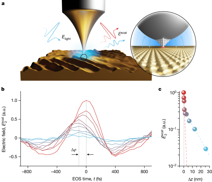
Deeper Inquiries
How can the authors' all-optical microscopy technique be further improved or extended to study even more complex quantum phenomena at the atomic scale?
The authors' all-optical microscopy technique can be further improved or extended by incorporating advanced signal processing algorithms to enhance the signal-to-noise ratio and extract more detailed information from the acquired data. Additionally, integrating machine learning algorithms for image reconstruction and analysis could help in identifying subtle quantum phenomena at the atomic scale. Furthermore, exploring different excitation wavelengths and polarization states of light could provide insights into specific quantum interactions and dynamics within materials. Collaborations with theoretical physicists to develop models that can predict and interpret the observed quantum phenomena would also be beneficial in advancing the technique for studying complex quantum systems.
What are the potential limitations or challenges in applying this technique to a wider range of materials or systems beyond the semiconducting van der Waals material showcased in the content?
One potential limitation in applying this technique to a wider range of materials is the variation in the optical properties and nonlinear responses of different materials. The technique may not be universally applicable to all materials, as some may exhibit weak nonlinearities or complex interactions that are challenging to capture with the current methodology. Additionally, the need for precise control and manipulation of the evanescent light fields at atomic scales could pose challenges when dealing with heterogeneous materials or systems with irregular surfaces. Another limitation could be the scalability of the technique to larger sample sizes or three-dimensional structures, as the current implementation seems tailored for nanoscale two-dimensional materials. Overcoming these challenges would require significant advancements in experimental design, theoretical modeling, and computational simulations to adapt the technique to a broader range of materials and systems.
What other emerging fields or applications could benefit from the unprecedented spatial and temporal resolution enabled by this all-optical microscopy approach, beyond the examples provided in the content?
The unprecedented spatial and temporal resolution enabled by this all-optical microscopy approach could benefit various emerging fields and applications. In the field of quantum computing, the ability to monitor and control quantum dynamics at atomic scales could aid in the development of quantum processors and quantum communication technologies. In the study of biological systems, this technique could provide insights into molecular interactions, protein dynamics, and cellular processes with unparalleled detail. Furthermore, in the field of materials science, the technique could revolutionize the design and characterization of novel materials with tailored quantum properties for applications in electronics, photonics, and energy storage. Additionally, the technique could find applications in ultrafast spectroscopy, quantum information processing, and nanophotonics, opening up new avenues for exploring and manipulating quantum phenomena at the atomic level.
0
Visualize This Page
Generate with Undetectable AI
Translate to Another Language
Scholar Search
Products | Resources
© 2024 by Linnk AI