
Sign In
insight - Computer hardware - # Vertical Integration of 2D Semiconductor Devices for Complementary Logic
Polarity Engineering and 3D Integration of 2D Complementary Logic Circuits
Core Concepts
Vertical three-dimensional integration of two-dimensional (2D) semiconductors enables scaling up logic layers, but the lack of controllable doping in 2D materials has impeded the development of complementary logic circuits. This work demonstrates a novel approach to engineer the carrier polarity in 2D semiconductors like MoS2 through van der Waals interfacial coupling, enabling the realization of vertically integrated complementary logic gates and circuits.
Abstract
The content discusses the challenges in scaling up logic layers in the z-axis through vertical three-dimensional integration of two-dimensional (2D) semiconductors. The key issue has been the lack of a controllable doping scheme, especially for p-doped 2D materials like WSe2 and MoS2.
The authors present a novel approach to overcome this challenge. By placing 2D semiconductors like MoS2 on top of a van der Waals (vdW) antiferromagnetic insulator chromium oxychloride (CrOCl), they demonstrate that the carrier polarity in MoS2 can be readily reconfigured from n-type to p-type through strong vdW interfacial coupling.
This polarity engineering enables the fabrication of high-performance transistors with room-temperature hole mobilities up to ~425 cm^2/V-s, on/off ratios reaching 10^6, and air-stable performance for over a year. Building on this, the authors further demonstrate vertically constructed complementary logic circuits, including inverters, NANDs, and SRAMs, using 2D semiconductor channels with engineered polarities.
The authors claim that their findings on polarity engineering and 3D integration of 2D complementary logic are robust and universal to various materials, potentially paving the way for future three-dimensional vertically integrated circuits based on 2D logic gates.
Van der Waals polarity-engineered 3D integration of 2D complementary logic - Nature
Stats
Hole mobility in engineered p-type MoS2 transistors: ~425 cm^2/V-s
On/off ratio of engineered p-type MoS2 transistors: up to 10^6
Air-stable performance of engineered p-type MoS2 transistors: over 1 year
Quotes
"By bringing transition metal dichalcogenides, such as MoS2, atop a van der Waals (vdW) antiferromagnetic insulator chromium oxychloride (CrOCl), the carrier polarity in MoS2 can be readily reconfigured from n- to p-type via strong vdW interfacial coupling."
"The consequential band alignment yields transistors with room-temperature hole mobilities up to approximately 425 cm2 V−1 s−1, on/off ratios reaching 106 and air-stable performance for over one year."
Key Insights Distilled From
by Yimeng Guo,J... at www.nature.com 05-29-2024
https://www.nature.com/articles/s41586-024-07438-5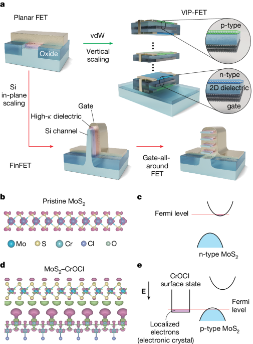
Deeper Inquiries
What other 2D semiconductor materials can be polarity-engineered using this van der Waals interface approach, and how do their properties and performance compare?
The van der Waals interface approach demonstrated in the study can be applied to various other 2D semiconductor materials beyond MoS2. For example, materials like WSe2, WS2, and MoSe2 can also be polarity-engineered using this method. By utilizing transition metal dichalcogenides (TMDs) atop van der Waals antiferromagnetic insulators, such as chromium oxychloride (CrOCl), the carrier polarity in these materials can be reconfigured from n-type to p-type. The properties and performance of these materials can vary based on their specific band structures, carrier mobilities, and interfacial interactions. Each material may exhibit different hole mobilities, on/off ratios, and stability characteristics when engineered for polarity using the vdW interface approach. It is essential to study and optimize the specific combinations of 2D semiconductors and insulators to achieve the desired performance metrics for different applications.
How scalable and manufacturable is the vertical integration of 2D complementary logic circuits demonstrated in this work, and what are the key challenges that need to be addressed for large-scale adoption?
The vertical integration of 2D complementary logic circuits showcased in the study shows promise for scalability and manufacturability. By stacking multiple layers of 2D materials with controlled carrier polarity using the vdW interface approach, complex logic circuits like inverters, NAND gates, and SRAMs can be constructed in the z-axis. This vertical integration enables the scaling up of logic layers, offering potential benefits in terms of compactness and performance. However, several challenges need to be addressed for large-scale adoption. These include optimizing the fabrication processes for precise layer alignment, ensuring uniform doping across the layers, improving interlayer contact resistance, and enhancing the overall yield and reproducibility of the devices. Additionally, the cost-effectiveness and compatibility of the manufacturing techniques with existing semiconductor processes need to be considered to enable widespread adoption of vertically integrated 2D complementary logic circuits.
Given the potential of 2D materials for energy-efficient electronics, how can the polarity engineering and 3D integration techniques be leveraged to develop novel low-power computing architectures and applications?
The polarity engineering and 3D integration techniques demonstrated in the study offer exciting opportunities for developing novel low-power computing architectures and applications using 2D materials. By tailoring the carrier polarity of 2D semiconductors through vdW interfaces, it is possible to design energy-efficient transistors with improved performance metrics. Leveraging these techniques, researchers can explore the development of ultra-low-power logic circuits, memory devices, and sensors that capitalize on the unique properties of 2D materials. The 3D integration of complementary logic circuits enables the creation of compact and power-efficient computing systems, paving the way for advancements in areas such as Internet of Things (IoT), wearable electronics, and edge computing. By further optimizing the polarity engineering methods and scaling up the 3D integration processes, innovative low-power computing architectures can be realized, driving the next generation of energy-efficient electronic devices and systems.
0
Products | Resources
Read more
- 다양성과-안정성-간의-근본적인-상충관계-다중-과제-벤치마크에-대한-통찰
- zero-shot-monocular-motion-segmentation-in-the-wild-by-combining-deep-learning-with-geometric-motion-model-fusion
- 単眼カメラによる野外での物体運動セグメンテーションのための深層学習と幾何学的運動モデルの融合
- 단일-카메라에서-심층-학습과-기하학적-모션-모델-융합을-통한-야생-환경의-제로-샷-모노큘러-모션-분할
- large-language-models-exhibit-biases-and-inconsistencies-as-automatic-evaluators
- 大規模言語モデルは一貫性がなく偏った評価者である
- 대형-언어-모델은-일관성이-없고-편향된-평가자이다
- leveraging-explainability-to-enhance-adversarial-evasion-attacks-on-windows-pe-malware-detectors
© 2024 by Linnk AI