
Sign In
Direct Growth of Graphene Nanoribbons in hBN Stacks for High-Performance Electronics
Core Concepts
Direct growth of high-quality graphene nanoribbons in hBN stacks enables the creation of high-performance electronic devices.
Abstract
The content discusses the direct growth of graphene nanoribbons (GNRs) in hexagonal boron nitride (hBN) stacks for high-performance electronics.
Van der Waals encapsulation in hBN stacks enhances electronic device performance.
Traditional methods of encapsulation are challenging and unscalable.
Transfer-free growth of GNRs in hBN stacks results in ultralong and ultranarrow structures.
Atomistic simulations reveal the mechanism of embedded growth in hBN layers.
Fabrication of GNR field-effect devices with excellent performance metrics.
Potential for bottom-up fabrication of high-performance electronic devices.
Graphene nanoribbons grown in hBN stacks for high-performance electronics - Nature
Stats
The as-grown embedded GNRs are ultralong (up to 0.25 mm), ultranarrow (<5 nm), and homochiral with zigzag edges.
GNR field-effect devices exhibit mobilities of up to 4,600 cm2 V–1 s–1 and on–off ratios of up to 106.
Quotes
"This paves the way for the bottom-up fabrication of high-performance electronic devices based on embedded layered materials."
Key Insights Distilled From
by Bosai Lyu,Ji... at www.nature.com 03-27-2024
https://www.nature.com/articles/s41586-024-07243-0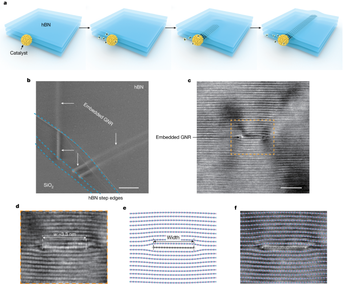
Deeper Inquiries
How can the direct growth of GNRs impact the scalability of electronic device production
The direct growth of graphene nanoribbons (GNRs) in hexagonal boron nitride (hBN) stacks can significantly impact the scalability of electronic device production. Traditional methods of achieving van der Waals encapsulation through mechanical transfer techniques are challenging to control, prone to contamination, and not easily scalable. By enabling transfer-free direct growth of GNRs in hBN stacks, the process becomes more efficient, reliable, and scalable. This advancement eliminates the need for complex transfer processes, reducing the risk of contamination and streamlining the production of high-quality GNR-based electronic devices. The ability to grow ultralong, ultranarrow, and homochiral GNRs directly in hBN stacks opens up new possibilities for large-scale manufacturing of high-performance electronic devices.
What challenges might arise in implementing transfer-free fabrication techniques on a larger scale
Implementing transfer-free fabrication techniques on a larger scale may pose several challenges. One significant challenge is ensuring uniformity and consistency in the growth of GNRs within hBN stacks across a large area. Controlling the growth parameters, such as temperature, pressure, and precursor concentration, becomes more complex when scaling up the production process. Additionally, maintaining the quality and integrity of the GNRs and hBN layers throughout the large-scale fabrication process is crucial to achieving high-performance electronic devices. Another challenge is optimizing the production throughput and efficiency to meet the demands of mass production while maintaining the desired device performance characteristics. Addressing these challenges will be essential for the successful implementation of transfer-free fabrication techniques on a larger scale.
How does the concept of van der Waals encapsulation in hBN stacks contribute to advancements in nanoelectronics
The concept of van der Waals encapsulation in hBN stacks plays a crucial role in advancing nanoelectronics by enabling the creation of high-performance electronic devices. By encapsulating two-dimensional materials like graphene within hBN layers, researchers can achieve ultrahigh-performance electronic devices with desirable properties. The van der Waals forces between the layers provide a stable and protective environment for the embedded materials, preventing external influences and enhancing their electronic properties. This encapsulation technique allows for precise control over the material interfaces, leading to improved device performance, reliability, and scalability. The ability to grow graphene nanoribbons directly in hBN stacks further enhances the potential for bottom-up fabrication of advanced electronic devices, paving the way for future innovations in nanoelectronics.
0
Visualize This Page
Generate with Undetectable AI
Translate to Another Language
Scholar Search
Products | Resources
© 2024 by Linnk AI