
ลงชื่อเข้าใช้
Leveraging Both Surfaces of Polar Semiconductor Wafers for Integrated Photonic and Electronic Devices
แนวคิดหลัก
The unique polarization properties of wide-bandgap semiconductors like gallium nitride (GaN) enable the use of both the cation and anion faces of the semiconductor wafer for distinct functional devices, unlocking new possibilities for integrated photonic, electronic, and acoustic capabilities.
บทคัดย่อ
The content discusses the potential of utilizing both surfaces of polar semiconductor wafers, such as gallium nitride (GaN), for functional devices. Unlike non-polar semiconductors like silicon, the broken inversion symmetry in wide-bandgap semiconductors like GaN leads to a large electronic polarization along a unique crystal axis. This makes the two surfaces of the semiconductor wafer (the cation or gallium face, and the anion or nitrogen face) substantially different in their physical and chemical properties.
In the past, the cation face of GaN has been predominantly used for photonic devices like light-emitting diodes (LEDs) and lasers. The anion face has also been used for electronic devices, but more recently has shown promise for high-electron-mobility transistors (HEMTs) due to favorable polarization discontinuities.
The key insight presented in this work is the introduction of "dualtronics", which demonstrates the possibility of making photonic devices on the cation face and electronic devices on the anion face of the same semiconductor wafer. This opens up new possibilities for integrating electronic, photonic, and acoustic properties on opposite faces of a single wafer, significantly enhancing the functional capabilities of this revolutionary semiconductor family.
Using both faces of polar semiconductor wafers for functional devices - Nature
สถิติ
The content does not provide any specific numerical data or metrics.
คำพูด
"This opens the possibility for making use of both faces of polar semiconductors in a single structure, in which electronic, photonic and acoustic properties can be implemented on opposite faces of the same wafer, markedly enhancing the functional capabilities of this revolutionary semiconductor family."
ข้อมูลเชิงลึกที่สำคัญจาก
by Len van Deur... ที่ www.nature.com 09-25-2024
https://www.nature.com/articles/s41586-024-07983-z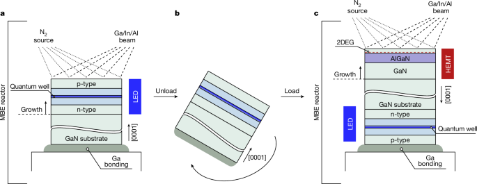
สอบถามเพิ่มเติม
What are the key technical challenges in realizing the "dualtronics" concept and integrating photonic and electronic devices on the opposite faces of a polar semiconductor wafer?
The realization of the "dualtronics" concept presents several key technical challenges. Firstly, the differing physical and chemical properties of the cation (gallium) and anion (nitrogen) faces of the polar semiconductor, gallium nitride (GaN), necessitate precise control over the growth and fabrication processes. Achieving uniform material quality and interface characteristics on both surfaces is critical, as any discrepancies could lead to performance degradation in the integrated devices.
Secondly, the integration of photonic and electronic devices requires advanced techniques for managing the polarization effects inherent in GaN. The large electronic polarization along the unique crystal axis can lead to polarization discontinuities that must be carefully engineered to optimize device performance. This involves developing new methods for doping, surface treatment, and layer deposition that can accommodate the distinct operational requirements of photonic and electronic components.
Additionally, thermal management poses a challenge, as the heat generated by electronic devices can adversely affect the performance of adjacent photonic devices. Effective thermal coupling and dissipation strategies must be implemented to ensure that both types of devices operate efficiently without interference.
Lastly, the design of interconnects and the overall architecture of the dual-device system must be carefully considered to facilitate seamless communication between the photonic and electronic components. This requires innovative approaches to circuit design and layout that can leverage the unique properties of both surfaces while maintaining high performance and reliability.
How might the ability to leverage both surfaces of polar semiconductor wafers impact the design and performance of future integrated circuits and systems?
Leveraging both surfaces of polar semiconductor wafers, such as GaN, could significantly enhance the design and performance of future integrated circuits and systems. By utilizing the cation face for photonic devices and the anion face for electronic devices, engineers can create highly integrated systems that combine the strengths of both domains. This dual functionality allows for the development of compact, multifunctional devices that can perform complex tasks more efficiently.
The integration of photonic and electronic components on a single wafer can lead to reduced signal loss and improved bandwidth, as optical interconnects can facilitate faster data transmission compared to traditional electrical connections. This is particularly beneficial for applications in telecommunications, data centers, and high-performance computing, where speed and efficiency are paramount.
Moreover, the ability to implement acoustic properties alongside electronic and photonic functionalities opens new avenues for sensor technologies and signal processing applications. The combination of these diverse functionalities on a single platform can lead to the development of novel devices such as optoelectronic sensors, integrated photonic circuits, and advanced communication systems that are more compact and energy-efficient.
Overall, the dualtronics approach could pave the way for next-generation integrated circuits that are not only more powerful but also capable of performing a wider range of functions, ultimately driving innovation in various fields, including consumer electronics, automotive systems, and smart infrastructure.
What other novel applications or device architectures could emerge from the unique polarization properties of wide-bandgap semiconductors beyond the examples discussed in the content?
The unique polarization properties of wide-bandgap semiconductors like GaN open the door to a variety of novel applications and device architectures beyond traditional photonic and electronic devices. One promising area is the development of advanced piezoelectric devices that exploit the polarization-induced strain in GaN. These devices could be used in energy harvesting applications, where mechanical energy is converted into electrical energy, or in sensors that detect changes in pressure or force.
Additionally, the polarization properties can be harnessed to create highly efficient terahertz (THz) sources and detectors. THz technology has numerous applications in imaging, spectroscopy, and communications, and leveraging the polarization characteristics of GaN could lead to the development of compact and efficient THz devices.
Another potential application is in the field of quantum technologies. The unique polarization states in GaN could be utilized to create quantum bits (qubits) for quantum computing or secure communication systems. The ability to manipulate polarization states with high precision could enable the development of robust quantum networks.
Furthermore, the integration of polarization-sensitive materials with GaN could lead to innovative optoelectronic devices, such as polarization-sensitive photodetectors and modulators, which could enhance the performance of optical communication systems by enabling advanced modulation schemes.
In summary, the unique polarization properties of wide-bandgap semiconductors like GaN not only enhance existing device functionalities but also pave the way for groundbreaking applications in energy harvesting, terahertz technology, quantum computing, and advanced optoelectronics, thereby expanding the horizons of semiconductor technology.
0
ลองดูภาพหน้านี้
สร้างด้วย AI ที่ตรวจจับไม่ได้
แปลเป็นภาษาอื่น
ค้นหางานวิจัย
เกี่ยวกับ
ผลิตภัณฑ์ | แหล่งข้อมูล
© 2024 by Linnk AI