
Увійти
Achieving Controllable p- and n-type Conductivity in High-Performance Perovskite Semiconductors
Основні поняття
Reliable control of p- and n-type conductivity in perovskite semiconductors, enabling high-performance optoelectronic devices.
Анотація
The article discusses the achievement of controllable p- and n-type conductivity in wide-bandgap perovskite semiconductors, which is crucial for modern electronics. Typically, doping of electron-accepting and electron-donating elements is used to achieve p- and n-type behaviors in semiconductors like silicon and gallium nitride. However, for the emerging class of halide perovskite semiconductors, reliable mechanisms for controlling charge conduction while maintaining high optoelectronic qualities were not yet discovered.
The researchers report that by incorporating a phosphonic acid molecular dopant with strong electron-withdrawing abilities, they were able to adjust the p- and n-type characteristics in a perovskite semiconductor. The resultant carrier concentrations exceeded 1013 cm−3 for both p- and n-type samples, with Hall coefficients ranging from −0.5 m3 C−1 (n-type) to 0.6 m3 C−1 (p-type). Importantly, the transition from n- to p-type conductivity was achieved while retaining high photoluminescence quantum yields of 70–85%.
The controllable doping in the emissive perovskite semiconductor enabled the demonstration of ultrahigh brightness (more than 1.1 × 10⁶ cd m−2) and exceptional external quantum efficiency (28.4%) in perovskite light-emitting diodes with a simple architecture.
Controllable p- and n-type behaviours in emissive perovskite semiconductors - Nature
Статистика
Carrier concentrations more than 1013 cm−3 for both p- and n-type samples.
Hall coefficients ranging from −0.5 m3 C−1 (n-type) to 0.6 m3 C−1 (p-type).
Photoluminescence quantum yields of 70–85% maintained.
Perovskite light-emitting diodes demonstrated ultrahigh brightness (more than 1.1 × 10⁶ cd m−2) and exceptional external quantum efficiency (28.4%).
Цитати
"Reliable control of the conductivity and its polarity in semiconductors is at the heart of modern electronics1,2,3,4,5,6,7, and has led to key inventions including diodes, transistors, solar cells, photodetectors, light-emitting diodes and semiconductor lasers."
"Importantly, the transition from n- to p-type conductivity was achieved while retaining high photoluminescence quantum yields of 70–85%."
Ключові висновки, отримані з
by Wentao Xiong... о www.nature.com 09-11-2024
https://www.nature.com/articles/s41586-024-07792-4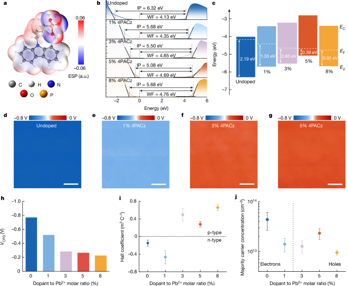
Глибші Запити
How can the doping techniques developed in this work be extended to other perovskite material systems to achieve similar control over conductivity?
The doping techniques demonstrated in this study can be extended to other perovskite material systems by employing similar molecular dopants with strong electron-withdrawing or electron-donating properties. By carefully selecting dopants that can effectively modify the electronic structure of various perovskite compositions, researchers can achieve tailored p- and n-type conductivity. Additionally, the incorporation of different phosphonic acid derivatives or other organic dopants could be explored to optimize carrier concentrations and enhance the stability of the perovskite lattice. Furthermore, the methodology of adjusting the Fermi level through controlled doping can be applied to other halide perovskites, allowing for the fine-tuning of their optoelectronic properties. This approach could also be adapted to hybrid perovskite systems, where the interplay between organic and inorganic components may yield unique conductivity characteristics. Overall, the principles of molecular doping and the resulting charge carrier modulation can be generalized across various perovskite materials, paving the way for a broader range of applications in electronics and optoelectronics.
What are the potential limitations or challenges in scaling up the fabrication of these highly doped perovskite semiconductors for practical device applications?
Scaling up the fabrication of highly doped perovskite semiconductors presents several challenges. One significant limitation is the uniformity of doping across large-area substrates, which is crucial for ensuring consistent electrical and optical properties in devices. Achieving homogenous distribution of dopants while maintaining the structural integrity of the perovskite lattice can be difficult, particularly in large-scale production. Additionally, the stability of the doped perovskite materials under operational conditions is a concern, as the incorporation of dopants may affect the material's resistance to moisture, heat, and light degradation. Another challenge lies in the compatibility of the doping process with existing fabrication techniques used in the semiconductor industry, which may require modifications to standard processes to accommodate the unique properties of perovskite materials. Finally, the economic feasibility of producing highly doped perovskite semiconductors at scale must be considered, as the cost of high-purity dopants and the complexity of the doping process could impact the overall viability of these materials for commercial applications.
Given the exceptional optoelectronic properties demonstrated, what other types of high-performance devices could be enabled by this controllable doping approach in perovskite materials?
The controllable doping approach in perovskite materials could enable a wide range of high-performance devices beyond light-emitting diodes (LEDs). For instance, the ability to finely tune p- and n-type conductivity could lead to the development of highly efficient perovskite-based solar cells, where optimized charge transport and collection can significantly enhance power conversion efficiencies. Additionally, this doping technique could be applied to create advanced photodetectors with improved sensitivity and response times, making them suitable for applications in imaging and sensing technologies. Furthermore, the exceptional optoelectronic properties of doped perovskites could facilitate the fabrication of high-performance laser diodes and semiconductor amplifiers, which are essential for telecommunications and data transmission. The versatility of this doping strategy also opens avenues for the development of novel electronic devices, such as transistors and memory elements, that leverage the unique properties of perovskite materials for next-generation electronic applications. Overall, the controllable doping of perovskites holds great promise for advancing various fields, including renewable energy, optoelectronics, and information technology.
0
Візуалізувати цю сторінку
Згенерувати за допомогою Undetectable AI
Перекласти іншою мовою
Пошук у Scholar
Продукти | Ресурси
© 2024 by Linnk AI