
Sign In
Automated Probing and Characterization of Spin Qubit Devices Across 300-mm Wafers for Scalable Quantum Computing
Core Concepts
Developing a scalable fabrication and testing process for spin qubit devices to enable the realization of fault-tolerant quantum computers.
Abstract
The content discusses the challenges in building a fault-tolerant quantum computer, which requires integrating millions of physical qubits in a single processor. Spin qubits based on electrons in silicon have shown impressive control fidelities, but have historically faced issues with yield and process variation.
The authors present a testing process using a cryogenic 300-mm wafer prober to collect high-volume data on the performance of hundreds of industry-manufactured spin qubit devices at 1.6 K. This automated measurement system enables fast feedback to optimize the CMOS-compatible fabrication process, leading to high yield and low process variation.
The authors analyze the random variation in single-electron operating voltages across the full wafers and find that the optimized fabrication process results in low levels of disorder at the 300-mm scale. These results demonstrate the advances that can be achieved by applying CMOS-industry techniques to the fabrication and measurement of spin qubit devices, which is a crucial step towards realizing scalable quantum computers.
Probing single electrons across 300-mm spin qubit wafers - Nature
Stats
The testing was performed at a temperature of 1.6 K.
The authors investigated the transitions of single electrons across full 300-mm wafers.
Quotes
"Building a fault-tolerant quantum computer will require vast numbers of physical qubits."
"Spin qubits1,4,5 based on electrons in Si have shown impressive control fidelities6,7,8,9 but have historically been challenged by yield and process variation10,11,12."
"Together, these results demonstrate the advances that can be achieved through the application of CMOS-industry techniques to the fabrication and measurement of spin qubit devices."
Key Insights Distilled From
by Samuel Neyen... at www.nature.com 05-01-2024
https://www.nature.com/articles/s41586-024-07275-6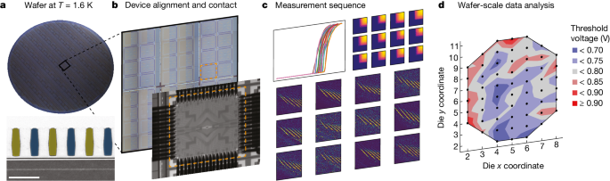
Deeper Inquiries
What are the specific CMOS-industry techniques that were applied to the fabrication and measurement of the spin qubit devices, and how can they be further improved?
In the context of spin qubit devices, specific CMOS-industry techniques that were applied include high-volume data collection using a cryogenic 300-mm wafer prober, automation of measurements for operating points of spin qubits, and analysis of single-electron transitions across full wafers. These techniques enable efficient device screening, optimization of fabrication processes, and improvement of statistical metrics such as qubit yield and voltage variation. To further enhance these techniques, advancements in wafer prober technology for even higher throughput testing, automation of more complex measurements for in-depth characterization, and integration of machine learning algorithms for real-time data analysis could be explored.
How do the findings on low disorder and process variation at the 300-mm scale compare to the challenges faced at smaller scales, and what are the implications for scaling up to larger wafer sizes?
The findings of low disorder and process variation at the 300-mm scale represent a significant advancement compared to the challenges faced at smaller scales. Historically, spin qubit devices have been plagued by yield and process variation issues, which hindered their scalability. The implications of achieving low disorder and process variation at the 300-mm scale are promising for scaling up to larger wafer sizes. This indicates that the optimized fabrication process is capable of maintaining consistency and quality across a larger surface area, which is crucial for integrating millions of qubits in a single processor. It suggests that with further refinement and optimization, the fabrication process can be scaled up to meet the demands of building fault-tolerant quantum computers with vast numbers of physical qubits.
How can the insights from this work on spin qubits be leveraged to advance the development of other qubit technologies, such as superconducting or topological qubits, towards scalable quantum computing?
The insights gained from the work on spin qubits, particularly in optimizing fabrication processes, improving yield, and reducing process variation, can be leveraged to advance the development of other qubit technologies like superconducting or topological qubits towards scalable quantum computing. By applying similar CMOS-industry techniques to these qubit technologies, researchers can streamline fabrication processes, enhance device testing methodologies, and increase overall efficiency. Lessons learned from addressing yield and process variation challenges in spin qubits can be translated to improve the scalability and reliability of superconducting or topological qubits, paving the way for the realization of large-scale, fault-tolerant quantum computers.
0
Products | Resources
Read more
- veclip-improving-clip-training-with-visual-enriched-captions
- understanding-domain-generalization-a-noise-robustness-perspective-at-iclr-2024
- グラフ分解学習に基づく多要素時空間予測
- ai-hazard-management-a-framework-for-systematic-ai-risk-management
- 直接かつ正確な情報を提供する効率的でダイナミックなステップ配置とローリングコンタクトによる効率的な動き
- 大規模言語モデルを活用したモバイルエッジコンピューティングシステムにおけるユーザー関連性とリソース割り当てについての研究
- tinympc-model-predictive-control-on-resource-constrained-microcontrollers
- veloの4000-tpu月の価値を評価-学習された最適化手法のスケーリングはそれだけの価値があるか-
© 2024 by Linnk AI