
Sign In
Discovery of Spontaneously Formed Magnesium-Intercalated Gallium Nitride Superlattices with Exceptional Strain and Unique Electronic Properties
Core Concepts
Spontaneous formation of two-dimensional magnesium-intercalated gallium nitride superlattices with exceptional uniaxial compressive strain and unique electronic properties.
Abstract
The content describes the discovery of a novel material system - magnesium (Mg)-intercalated gallium nitride (GaN) superlattices. These superlattices form spontaneously by annealing a metallic Mg film on GaN at atmospheric pressure, marking the first instance of a two-dimensional metal intercalated into a bulk semiconductor.
The key highlights are:
The Mg monolayers are intricately inserted between several monolayers of hexagonal GaN, in an interstitial intercalation process.
This process induces substantial uniaxial compressive strain perpendicular to the Mg-intercalated layers, with the GaN layers exhibiting an exceptional elastic strain exceeding -10% (equivalent to a stress of more than 20 GPa).
The strain alters the electronic band structure and greatly enhances hole transport along the compression direction.
The Mg sheets also induce a unique periodic transition in GaN polarity, generating polarization-field-induced net charges.
These characteristics offer fresh insights into semiconductor doping, conductivity enhancement, and elastic strain engineering of nanomaterials and metal-semiconductor superlattices.
Observation of 2D-magnesium-intercalated gallium nitride superlattices - Nature
Stats
The GaN layers in the Mg-intercalated GaN superlattices exhibit an exceptional elastic strain exceeding -10% (equivalent to a stress of more than 20 GPa).
Quotes
"To our knowledge, this marks the first instance of a two-dimensional metal intercalated into a bulk semiconductor, with each Mg monolayer being intricately inserted between several monolayers of hexagonal GaN."
"Consequently, the GaN layers in the Mg-intercalated GaN superlattices exhibit an exceptional elastic strain exceeding −10% (equivalent to a stress of more than 20 GPa), among the highest recorded for thin-film materials."
Key Insights Distilled From
by Jia Wang,Wen... at www.nature.com 06-05-2024
https://www.nature.com/articles/s41586-024-07513-x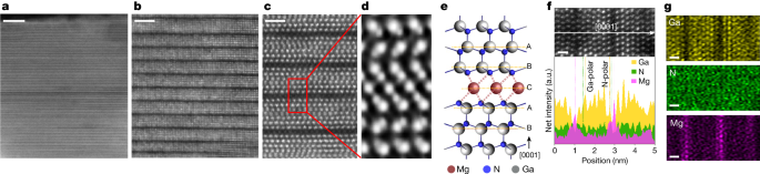
Deeper Inquiries
What other two-dimensional metals could be intercalated into bulk semiconductors, and what unique properties might they exhibit?
Intercalation of two-dimensional metals into bulk semiconductors presents a fascinating avenue for exploring novel material properties. Metals like aluminum, titanium, and zinc could potentially be intercalated into semiconductors like silicon or germanium. Each metal-semiconductor combination would offer unique properties based on their atomic structures and electronic configurations. For instance, aluminum intercalation could introduce significant tensile strain due to its larger atomic size, potentially altering the band structure of the semiconductor. Titanium, known for its strong bonding characteristics, could form stable interfaces with semiconductors, enhancing charge carrier mobility. Zinc, with its ability to exhibit multiple oxidation states, might introduce interesting electronic states within the semiconductor bandgap, leading to tailored optoelectronic properties.
How could the periodic polarity transition induced by the Mg sheets be leveraged for novel electronic or optoelectronic device applications?
The periodic polarity transition induced by Mg intercalation in GaN superlattices opens up exciting possibilities for novel electronic and optoelectronic device applications. One potential application could be in the development of field-effect transistors (FETs) with enhanced carrier mobility. By harnessing the polarization-field-induced net charges generated by the polarity transition, FETs could exhibit improved performance characteristics, such as higher on-off ratios and faster switching speeds. Additionally, the controlled manipulation of polarity in GaN could be utilized in the design of advanced photodetectors with tunable spectral response. The unique charge distribution resulting from the polarity transition may enable the creation of photodetectors with enhanced sensitivity and selectivity across different wavelengths, paving the way for next-generation optoelectronic devices.
What other potential applications could this Mg-intercalated GaN superlattice system have, beyond the insights into semiconductor doping and strain engineering discussed in the content?
The Mg-intercalated GaN superlattice system holds promise for a diverse range of applications beyond semiconductor doping and strain engineering. One intriguing possibility is the utilization of these superlattices in high-performance sensors. The exceptional elastic strain induced by Mg intercalation could be leveraged to create highly sensitive strain sensors capable of detecting minute mechanical deformations. Moreover, the unique electronic band structure resulting from the intercalation process could enable the development of ultrafast and low-power electronic devices, such as high-frequency transistors and logic gates. Furthermore, the strain-engineered GaN layers in the superlattices may find applications in the field of quantum technologies, where precise control over material properties is crucial for quantum information processing and quantum communication protocols.
0
Products | Resources
Read more
- computational-decomposition-and-composition-technique-for-approximate-solution-of-nonstationary-problems
- adaptive-constellation-multiple-access-für-wireless-systeme-jenseits-von-5g
- modeling-uncertainty-in-gaussian-splatting-for-novel-view-synthesis
- 유니파이드-용량-결과-자유-공간-광-통신-시스템의-감마-감마-대기-난류-채널에-대한
- lightweight-embeddings-for-graph-collaborative-filtering-efficient-parameter-optimization-for-improved-recommendations
- einheitliche-kapazitätsergebnisse-für-freiraum-optische-kommunikationssysteme-über-gamma-gamma-atmosphärische-turbulenzkanäle
- llms-mathematical-reasoning-in-financial-document-question-answering-evaluation
- enhanced-generative-recommendation-via-content-and-collaboration-integration
© 2024 by Linnk AI